
Page 40 - 半导体视界
P. 40
06 技术纵横 — 技术深度 Technology Panorama — Technical Depth 半导体视界 SEMICONDUCTOR HORIZONS 半导体视界 SEMICONDUCTOR HORIZONS 技术纵横 — 技术深度 Technology Panorama — Technical Depth 06
前沿技术多点突破 原始创新厚积薄发 岳麓山工业创新中心段曦东团队破局二维半导体
中国半导体研究与工艺跃迁全球视野
文 / 田也 , 中国国际科技促进会半导体产业发展分会 , 宣传部主任
Multiple Breakthroughs in Frontier Technologies, Original Innovations Ready to Emerge
China’s Semiconductor Research and Process Leap: A Global Perspective
By Tian Ye, Director of the Propaganda Department of the Development Of Semiconductor Industrial Branch of the 来源:岳麓山工业创新中心微信公众号
China International Association for Promotion of Science and Technology
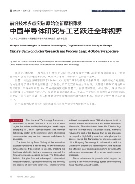
1L-SnS2/2L-WSe2 vdWH 短沟道 FET 的超高 Ion 与超低 Ron 特性
本期《技术纵横——技术深度》聚焦于 2025年夏季我国半导体与前沿科技领域涌现的一系列
重大原始创新与关键技术突破,展现出从材料、器件到工艺的全面进展。 6 月 12 日, 国 际 权 威 期 刊《Science》 在 线 发 表 岳 1.49×1014 cm–2 的超高二维空穴浓度。高空穴浓度使
岳麓山实验室段曦东团队于《Science》发表二维半导体超掺杂新策略,突破传统介电极限, 麓 山 工业 创 新 中心、 湖 南 大 学化 学 化 工 学院、 二 维 材料 p 型 2D 晶体 管展现 出优异 性能, 其最低 源漏 接触电 阻
为高性能电子器件开辟全新路径;长春应化所开发双自由基分子材料,大幅提升钙钛矿电池效率 湖 南 省 重 点 实 验 室 段 曦 东 教 授 团 队 完 成 的、 具 有 普适 性 (RC) 低 至 0.041kΩ · μm, 最 高 开 态 电 流 密 度(Ion)
与稳定性;平煤神马实现 8N8超高纯度碳化硅粉体量产,打破国际垄断。与此同时,深圳平台激 的栅极调控能带调制超掺杂策略的最新研究成果。 高达 2.30mA/μm。
光剥离技术达到国际先进水平,显著降低 SiC器件成本;中山大学研制出高保真度量子纠缠光源, 段曦东教授团队使用单层二硫化锡(1L-SnS2)与 研究成果成功实现了 2DSCs 中超高的 n2D,超低
双层二硒化钨(2L-WSe2)构建具有 III 型能带排列的 RC 与 Ron 以及创纪录的高 Ion。这为调控二维半导体
为光量子芯片奠定基础;华工科技联合中科大揭示紫外激光退火机理,推动化合物半导体工艺自
范德华异质结构(vdWHs)。背栅偏置电压(Vgs)能 中的载流子浓度提供了一种超越传统电介质限制的能带
主化。
够 对 层 间 电 荷 转 移 掺 杂 进 行 有 效 调 制, 实 现 了 超 过典 型 调制掺杂方法,为未来高性能 2D 电子器件的开发开辟了
这些成果为构建自主可控技术体系和未来产业竞争力提供坚实支撑。
介电击穿的最大静电掺杂极限的超掺杂,获得了高达 新途径。
Abstract This issue of Technology Panorama · achieved mass production of 8N8 ultra-high-purity silicon
Technology in Depth focuses on a series of major carbide powder, breaking the international monopoly.
original innovations and key technological breakthroughs Meanwhile, Shenzhen-based laser lift-off technology 我国科学家实现新型半导体光伏研发突破
emerging in China’s semiconductor and frontier reached internationally advanced levels, markedly
technology sectors in the summer of 2025, showcasing reducing the cost of SiC devices; Sun Yat-sen University
comprehensive progress from materials and devices to developed a high-fidelity quantum entangled photon
processes. source, laying the foundation for photonic quantum
The team led by Duan Xidong at the Yuelushan chips; Huagong Technology, in collaboration with the
Laboratory published a new strategy for two-dimensional University of Science and Technology of China, revealed
semiconductor hyperdoping in Science, breaking the the ultraviolet laser annealing mechanism, advancing the
traditional dielectric limit and opening a new path for independent development of compound semiconductor
high-performance electronic devices. The Changchun processes.
Institute of Applied Chemistry developed double-radical These achievements provide solid support for
molecular materials, significantly enhancing the efficiency building a self-reliant technology system and enhancing
and stability of perovskite solar cells. Pingmei Shenma future industrial competitiveness. 来源:人民日报海外版 2025 年 07 月 03 日 第 09 版
https://paper.people.com.cn/rmrbhwb/pc/content/202507/03/
content_30084386.html
40 Volume 1,lssue 1,2025 Volume 1,lssue 1,2025 41